Solbourne Hardware
Additional information about Solbourne hardware. I apologize in advance for the terrible image quality.
K-bus
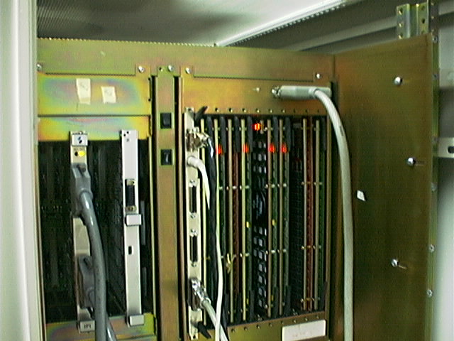
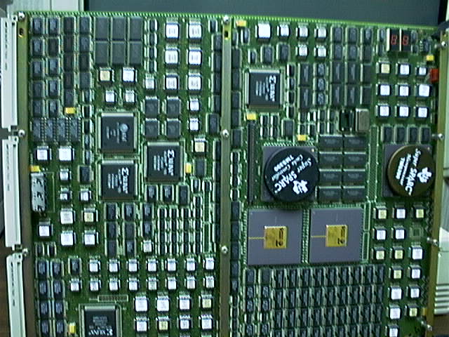
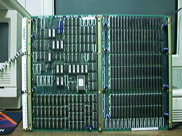
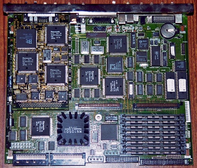
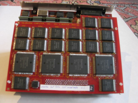
The largest (rack-mount) system supported 11 K-bus slots and 7 VME slots. The IO board and one memory board were mandatory. Only 8 CPU boards were supported officially but the system and OS would work with 9 CPUs. The Series 6 CPU used TI's "Viking" Processor and companion 1 MB L2 cache controller running in Mbus mode with a 16 MB L3 cache. The Series 6E CPU board ran at 40 MHz. The board had one datapath ASIC for the L3 cache, 5 FPGAs and countless PALs. This board may have been the most complex design Solbourne did.
K-bus was essentially designed around timing for the DRAM-based memory boards. It even included a transaction to cause all memory boards to refresh (note the big electrolytic capacitor on board to deal with that). When I designed the monochrome frame buffer I briefly considered storing data in main memory and using DMA to copy it to the screen in realtime. At the time 108 MB/sec seemed like a huge number. At the highest resolution of 1600 x 1280 pixels I would have needed less than 20 MB/sec for a 72 Hz refresh rate. It would have been a terrible design mistake because we needed every MB/sec we could get for the CPUs. It was an idea ahead of its time.
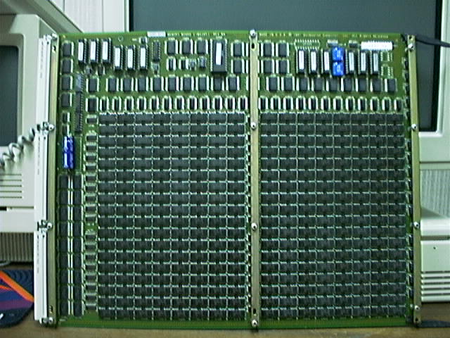
A company in Texas actually reversed engineered a Solbourne memory board and began selling clone boards. Solbourne eventually reached an agreement with this company and they produced a 1 GB memory board for Solbourne which sold for a phenomenal amount of money.
A company in Texas actually reversed engineered a Solbourne memory board and began selling clone boards. Solbourne eventually reached an agreement with this company and they produced a 1 GB memory board for Solbourne which sold for a phenomenal amount of money.
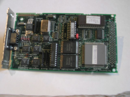
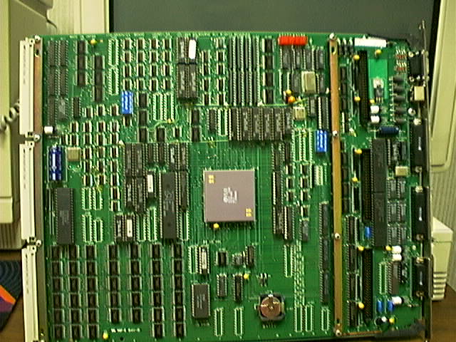
The IO board was the kitchen-sink for the system. It contained an ASIC bridge to VME, ethernet, monochrome graphics, two serial ports, keyboard/mouse ports, RTC, and parameter EEPROM (CMOS in PC terms). It was also the buggiest part of the system due to the asynchronous nature of VME. Over the years it was reved countless times (mainly because the ASIC designer had left and no-one wanted to try to fix bugs in the ASIC itself). Supporting it was a thankless job. There are countless stories about the iconoclastic engineers like Randy Willig who designed and supported the board and the ASIC.
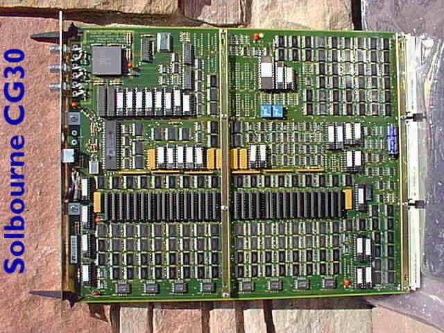
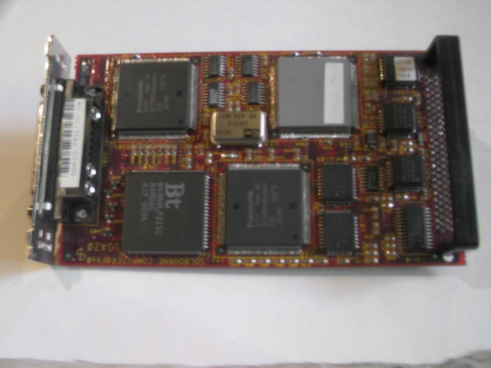
The CG30 was the first accelerated color graphics board. The ROP chips are along the bottom with the datapath above. We included a second keyboard/mouse port on this board and could support multiple users on one machine. We also included a Brooktree RAMDAC with a built-in hardware cursor which was used by X11 but not any of Sun's software. The Western Research Lab at DEC had published an article claiming that raster-op functions were all the acceleration a 2D graphics board really needed and in a way they were right. This board was plenty fast for its day (although I remember it had poor performance in early experiments with real-time video).
Desktop Products
The desktop family was based on the Solbourne and Matsushita designed KAP SPARC microprocessor running at 33 MHz. Both systems shared the same motherboard with 4 Solbourne designed ASICs. The S4000 was designed by Solbourne and the S3000 designed by Matsushita for the smaller desks in Japan. The S3000 had a custom SBus monochrome graphics card that drove a 1152x900 pixel plasma display. It actually wasn't as bad to look at as you might think from my poor photo. The KAP microprocessor was a huge disappointment. In an effort to make the S4000 family more competitive a really smart engineer named Doug Dushatko figured out how to attach a L2 cache to KAP and we designed that onto a small board that would plug into the existing KAP socket. After a huge amount of arm wrestling/pleading we got Matsushita to qualify KAP at the blistering rate of 36 MHz (the original target was 40 MHz). The new product was called the S4000DX (or S4100). My roommate at the time lead the S4000 effort while I led the graphics effort. Competition between us for resources pretty much ended our friendship and that's too bad. I was young and had a lot to learn.
S3000 Plasma Display
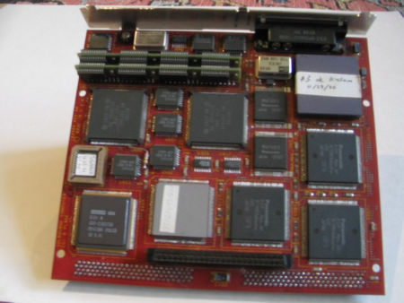
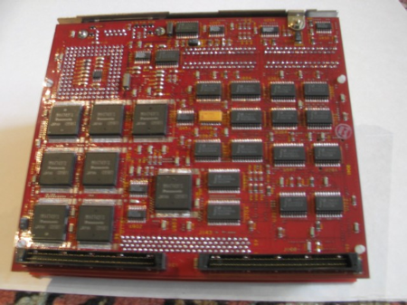
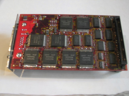
The SGA40 was a 3D graphics board at 1280x1024 pixel resolution with 8 color plans, 2 overlay planes and a 16-bit z-buffer. It interfaced to the system through a DMA SBus controller that had built-in virtual-to-physical address translation so the graphics board could access graphics data structures in user-land applications. That was a pain for the kernel to maintain although it's common now. It used two AT&T DSP32C DSPs at 25 MFLOPS each for command processing and the 3D graphics pipeline. The rendering pipeline used a graphics controller that computed polygon data (and 2D operations) and drove a set of parallel datapath chips, one chip for each PIPRAM. The PIPRAMs had 16-bit synchronous data buses and the rendering pipeline ran at 16.67 MHz. The RAMDAC also included a hardware cursor. The architecture could scale to dual-buffered 24-bit frame buffers but that board (destined for K-bus) was never completed.
SGA20 used the graphics control chip, two data path chips and eight PIPRAMs to provide a 1152x900 pixel 8-bit 2D accelerated display. The system architecture was designed around the PIPRAM 1280x1024 array pixel array. Sun's direct frame buffer access model required a linear array of memory so we used two 64Kx8 ROMs to remap the address as it came in when software accessed the frame buffer directly. The board performed pretty well although it was a slave-only device. It had pipelined writes and full 2D acceleration. PIPRAM supported a 32x32 tile fill function so rectangular fills (e.g. screen clears) were incredibly fast. This board went from the first planning meeting to running with Sun's Pixrects and our own X11 in 2 weeks, 2 days. We paid out the ear for the proto boards (which were hand delivered to my house on a Saturday afternoon). The only issue was contention in some SBus data buffers that was quickly fixed with a PAL change. This board would have been so much cheaper if we had designed using commercial VRAM.
The monochrome board was software compatible with the K-bus version (just raw pixel data) but used an ASIC designed in Japan to interface with SBus. It used similar ECL circuitry to drive the output to the monitor (100 MHz dot clock). Notice the two PIPRAMs. I think this board could be configured to support a higher resolution with a higher dot clock but that product was never marketed.